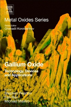
Gallium Oxide Technology, Devices and Applications Metal Oxides Series
Coordonnateurs : Pearton Stephen, Ren Fan, Mastro Michael

Gallium Oxide: Technology, Devices and Applications discusses the wide bandgap semiconductor and its promising applications in power electronics, solar blind UV detectors, and in extreme environment electronics. It also covers the fundamental science of gallium oxide, providing an in-depth look at the most relevant properties of this materials system. High quality bulk Ga2O3 is now commercially available from several sources and n-type epi structures are also coming onto the market. As researchers are focused on creating new complex structures, the book addresses the latest processing and synthesis methods.
Chapters are designed to give readers a complete picture of the Ga2O3 field and the area of devices based on Ga2O3, from their theoretical simulation, to fabrication and application.
1. Introduction and Overview
Part 1: Technology of Ga2O3 2. Bulk Growth of Ga2O3 by Edge-Fed Ribbon method 3. Progress in MOCVD growth of Ga2O3 4. CVD of different Ga2O3polymorphs and their applications 5. Pulsed laser deposition of aluminum gallium oxides for deep-UV detector applications 6. Dry Etching of Ga2O3 7. Ga2O3 -based nanostructures 8. Doping of Ga2O3
Part 2: Properties 9. Structural, electrophysical and optical properties of Ga2O3 10. First-principles modeling of sesquioxide semiconductors 11. Schottky Contacts to Ga2O3 12. Ohmic contacts to Ga2O3 13. Surface Properties of Ga2O3 14. Deep Traps in Ga2O3 15. Radiation Damage in Ga2O3
Part 3: Applications 16. Novel Solar-Blind Photodetectors and FETs Using Ga2O3 Exfoliated Flakes 17. FINFETs and Power MOSFETs 18. Power Ga2O3 Rectifiers 19. UV detectors 20. Ga2O3-based gas sensors 21. Photocatalysis (photocatalytic conversion CO2, etc.) 22. Transparent conductive oxides (amorphous Ga2O3 films)
Materials Scientists (Researchers and Engineers), Physicists, and Chemists in academia and industry r&d
Fan Ren was responsible for high-speed device development in the compound semiconductor area at Bell Labs prior to joining UF in 1998. He has over 22 years’ experience in device fabrication of state-of-the-art electronic devices. He is a Fellow of IEEE, ECS, SPIE, MRS, APS and AVS. Prof. Ren will be responsible for electrical measurements, dielectric depositions, contact formation and some of the data interpretation. Prof. Ren also has an extensive background in radiation effects and in the development of wide bandgap materials and devices and demonstrated the first Ga2O3/Gd2O3 insulated gate n-channel enhancement-mode InGaAs MOSFET's.
Michael Mastro’s research interests are in fabrication and modeling physics of high power transistors as well as light emitting, photonic crystal, plasmonic, metamaterial, and photovoltaic devices, fabrication of nano-structured devices, development of numerical models and neural network algorithms to describe nano-scale semiconductor physics. He is the co-editor of the very popular book “III-V Compound Semiconductors: Integration with Silicon-Based Microelectronics published by CRC Press. Michael will coordinate our efforts with NRL, help supply samples and facilitate additional characterization of irradiated structures.
- Provides an overview of the advantages of the gallium oxide materials system, the advances in in bulk and epitaxial crystal growth, device design and processing
- Reviews the most relevant applications, including photodetectors, FETs, FINFETs, MOSFETs, sensors, catalytic applications, and more
- Addresses materials properties, including structural, mechanical, electrical, optical, surface and contact
Date de parution : 10-2018
Ouvrage de 507 p.
15x22.8 cm
Thèmes de Gallium Oxide :
Mots-clés :
Acceptors; Al2O3; Atomic density; Band offset; Bandgap; Carrier removal rate; Combinatorial material science; Compensation; Conduction band; Contact annealing; Contact resistance; Crystal orientations; CVD; Damage; Dangling bond; Defect structures; Defects; Diodes; Dry etching; Dynamic screening; Electron cyclotron resonance (ECR); Electron paramagnetic resonance; Electron transport; Electron-phonon interactions; Electrons; ɛ-Ga2O3; Fluorinated substances; Functional nanowires; Ga vacancy; Ga2O3; Gallium oxide; Gallium Oxide; Gamma rays; Gas sensor; Heteroepitaxy; Heterogeneous dispersion; Heterostructures; High power transistor; Homoepitaxy; Hydrogen; Indium gallium oxide; Inductively coupled plasma (ICP); Insecticide; Ion milling; Keywordβ-Ga2O3 nanobelt; Lattice damage; Luminescence property; MBE; Mechanical exfoliation; Metallization; Metalorganic chemical vapor deposition; Mobility; MOCVD; Molecular beam epitaxy; Monte Carlo simulations; MSM; Nanodevice; Nanostructure; Nanostructures; Nanowire; Nanowires; Negative differential conductivity; Neutrons; Ohmic contact; Optical characterization; Optical properties; Optical property; Phonon mode; Photocatalysis; Photocatalyst; Photocatalytic activity; Photodetector; Photodetectors; Photomineralization; Plasma etching; Plasmon-phonon coupling; Polymorphism; Polymorphs of Ga2O3; Power MOSFETs; Protons; Radiation damage; Reactive ion etching (RIE); Schottky; Schottky barrier heights; Schottky contact; Schottky contacts; Self-trapped hole; Semiconducting gallium oxide; Shallow donors; SiO2; Solar-blind; Solar-blind photodetector; Specific contact resistance; Sputtering; Structural properties; Theory of vibrational properties; Thermal evaporation; Toxicity; Transition-metal ions; UV photodetectors; UVC radiation; Valence band; Velocity saturation; Vibrational spectroscopy; Wide bandgap semiconductor; β-Ga2O3


