


Description
High-k Materials in Multi-Gate FET Devices
Science, Technology, and Management Series
Language: English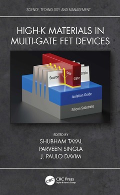
Subjects for High-k Materials in Multi-Gate FET Devices:
Keywords
Low Power VLSI; SCEs; FET; Oxide Semiconductor Field Effect Transistor; Field Effect Transistors; Multi-gate Devices; SRAM Cell; Gate Oxide; Equivalent Oxide Thickness; Gate Stack; Power Consumption; Gate Terminal; GIDL; MOSFET Device; MOS Transistor; Trap Charges; Flat Band Voltage; Steep Sub-threshold Slope; Carbon Nanotube FETs; Nanowire FET; Conventional MOSFET; Gate Drain Overlap; 6T SRAM Cell; Access Transistor; Sentaurus TCAD

Publication date: 09-2023
· 15.6x23.4 cm · Paperback
Publication date: 09-2021
· 15.6x23.4 cm · Hardback
Description
/li>Contents
/li>Biography
/li>
High-k Materials in Multi-Gate FET Devices focuses on high-k materials for advanced FET devices. It discusses emerging challenges in the engineering and applications and considers issues with associated technologies. It covers the various way of utilizing high-k dielectrics in multi-gate FETs for enhancing their performance at the device as well as circuit level.
- Provides basic knowledge about FET devices
- Presents the motivation behind multi-gate FETs, including current and future trends in transistor technologies
- Discusses fabrication and characterization of high-k materials
- Contains a comprehensive analysis of the impact of high-k dielectrics utilized in the gate-oxide and the gate-sidewall spacers on the GIDL of emerging multi-gate FET architectures
- Offers detailed application of high-k materials for advanced FET devices
- Considers future research directions
This book is of value to researchers in materials science, electronics engineering, semiconductor device modeling, IT, and related disciplines studying nanodevices such as FinFET and Tunnel FET and device-circuit codesign issues.
Chapter 1 Introduction to Multi-Gate FET Devices
Chapter 2 High-k Gate Dielectrics and Metal Gate Stack Technology for
Advance Semiconductor Devices: An Overview
Chapter 3 Influence of High-k Material in Gate Engineering and in
Multi-Gate Field Effect Transistor Devices
Chapter 4 Trap Charges in High-k and Stacked Dielectric
Chapter 5 Impact of High-k Dielectric on the Gate-Induced Drain
Leakage of Multi-Gate FETs
Chapter 6 Advanced FET Design Using High-k Gate Dielectric and
Characterization for Low-Power VLSI
Chapter 7 Simulation and Analysis of Gate Stack DG MOSFET with
Application of High-k Dielectric Using Visual TCAD
Chapter 8 Novel Architecture in Gate All-Around (GAA) MOSFET
with High-k Dielectric for Biomolecule Detection
Chapter 9 Asymmetric Junctionless Transistor: A SRAM
Performance Study
Chapter 10 Performability Analysis of High-k Dielectric-Based
Advanced MOSFET in Lower Technology Nodes
Index
Dr. Shubham Tayal is Assistant Professor, Department of Electronics and Communication Engineering, SR University, Warangal, India. He completed his Ph.D in VLSI from NIT, Kurukshetra. He has contributed 14 (10 - SCI/SCIE, 04 - Others) research papers in international journals, 2 research papers to IEEE Conferences, and 2 research papers to other national conferences. His research interests include simulation and modelling of multi-gate semiconductor devices, device-circuit co-design in digital/analog domain, and low power VLSI design.
Dr. Parveen Singla is Professor in Electronics & Communication Engineering, Department of Chandigarh Engineering College- Chandigarh Group of Colleges, Landran, Mohali, Punjab. He did his Bachelor of Engineering in Electronics & Communication Engineering with honors from Maharishi Dayanand University, Rohtak, Master in Technology in Electronics & Communication Engineering with honors from Kurukshetra University, Kurukshetra & PhD in Communication Systems from IKG Punjab Technical University, Jalandhar, India. He has 16 years of experience in the field of teaching and research. He has published more than 35 papers in various reputed journals and national and international conferences. He also organised more than 30 technical events for students in order to enhance their technical skills and received Best International Technical Event Organiser Award. He is the guest editor of various reputed journals. His interest area includes drone technology, wireless networks, smart antennas and soft computing.
Dr. J. Paulo Davim received his Ph.D. degree in Mechanical Engineering in 1997, M.Sc. degree in Mechanical Engineering (materials and manufacturing processes) in 1991, Mechanical Engineering degree (5 years) in 1986, from the University of Porto (FEUP), the Aggregate title (Full Habilitation) from the University of Coimbra in 2005 and the D.Sc. (Higher Doctorate) from London Metropolitan University in 2013. H
These books may interest you

Nanoscale Silicon Devices 71.13 €