Description
Crystal Growth and Evaluation of Silicon for VLSI and ULSI
Language: English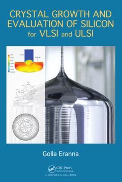
Subjects for Crystal Growth and Evaluation of Silicon for VLSI and ULSI:
Keywords
ULSI Circuit; Oxygen Precipitation; ULSI Processing; CZ Silicon; VLSI Processing; Silicon Wafer; Silicon Wafer Packing; Silicon Crystals; Silicon Wafer Preparation; Stacking Faults; Defects; Metallic Contamination; Impurities; Minority Carrier Lifetime; Resistivity; Silicon Melt; Silicon Wafers; Magnetic Eld; Silicon Ingots; Point Defects; Single-Crystal Silicon; Molten Silicon; Single Crystals; CZ Crystal; Integrated Circuit Fabrication; Pull Rate; Silicon Crystal Evaluation; Metallurgical Grade Silicon; Silicon Crystal Growth; Grown Crystal; Crystal Growth; Silicon; Metallic Impurities; ULSI; VLSI Technology; VLSI; Quartz Crucible; Silicon Surface; Electrochemical Society; Denuded Zone; Crystal Melt Interface; Melt Convection

Publication date: 12-2014
· 17.8x25.4 cm · Hardback
Publication date: 10-2016
· 17.8x25.4 cm · Paperback
Description
/li>Contents
/li>Readership
/li>Biography
/li>
Silicon, as a single-crystal semiconductor, has sparked a revolution in the field of electronics and touched nearly every field of science and technology. Though available abundantly as silica and in various other forms in nature, silicon is difficult to separate from its chemical compounds because of its reactivity. As a solid, silicon is chemically inert and stable, but growing it as a single crystal creates many technological challenges.
Crystal Growth and Evaluation of Silicon for VLSI and ULSI is one of the first books to cover the systematic growth of silicon single crystals and the complete evaluation of silicon, from sand to useful wafers for device fabrication. Written for engineers and researchers working in semiconductor fabrication industries, this practical text:
- Describes different techniques used to grow silicon single crystals
- Explains how grown single-crystal ingots become a complete silicon wafer for integrated-circuit fabrication
- Reviews different methods to evaluate silicon wafers to determine suitability for device applications
- Analyzes silicon wafers in terms of resistivity and impurity concentration mapping
- Examines the effect of intentional and unintentional impurities
- Explores the defects found in regular silicon-crystal lattice
- Discusses silicon wafer preparation for VLSI and ULSI processing
Crystal Growth and Evaluation of Silicon for VLSI and ULSI is an essential reference for different approaches to the selection of the basic silicon-containing compound, separation of silicon as metallurgical-grade pure silicon, subsequent purification, single-crystal growth, and defects and evaluation of the deviations within the grown crystals.
Introduction. Silicon: The Key Material for Integrated Circuit Fabrication Technology. Importance of Single Crystals for Integrated Circuit Fabrication. Different Techniques for Growing Single-Crystal Silicon. From Silicon Ingots to Silicon Wafers. Evaluation of Silicon Wafers. Resistivity and Impurity Concentration Mapping of Silicon Wafers. Impurities in Silicon Wafers. Defects in Silicon Wafers. Silicon Wafer Preparation for VLSI and ULSI Processing. Packing of Silicon Wafers.
Golla Eranna obtained his master’s degree from Sri Venkateswara University, Tirupati, India, with a top rank in the field of semiconductor physics. After that, he joined and received his Ph.D from the Indian Institute of Technology (IIT) Madras. Later, he moved to the IIT Kharagpur Microelectronics Centre. Dr. Eranna joined CEERI, Pilani, India, as a scientist and is currently a senior principal scientist. He became a professor under the Academy of Scientific and Innovative Research (CSIR, New Delhi), and regularly lectures on VLSI processing technology. He also maintains a full-fledged semiconductor device fabrication laboratory.