


Description
Vacuum Nanoelectronic Devices
Novel Electron Sources and Applications
Authors: Evtukh Anatoliy, Hartnagel Hans, Yilmazoglu Oktay, Mimura Hidenori, Pavlidis Dimitris
Language: English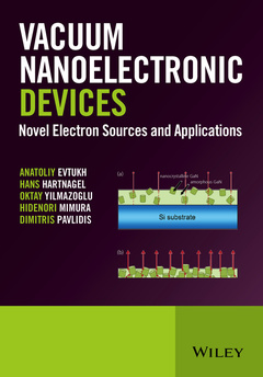
Subject for Vacuum Nanoelectronic Devices:
128.91 €
In Print (Delivery period: 14 days).
Add to cart the book of Evtukh Anatoliy, Hartnagel Hans, Yilmazoglu Oktay, Mimura Hidenori, Pavlidis Dimitris
512 p. · 17.5x25.2 cm · Hardback
Description
/li>Contents
/li>Biography
/li>
Introducing up-to-date coverage of research in electron field emission from nanostructures, Vacuum Nanoelectronic Devices outlines the physics of quantum nanostructures, basic principles of electron field emission, and vacuum nanoelectronic devices operation, and offers as insight state-of-the-art and future researches and developments.
This book also evaluates the results of research and development of novel quantum electron sources that will determine the future development of vacuum nanoelectronics. Further to this, the influence of quantum mechanical effects on high frequency vacuum nanoelectronic devices is also assessed.
Key features:
? In-depth description and analysis of the fundamentals of Quantum Electron effects in novel electron sources.
? Comprehensive and up-to-date summary of the physics and technologies for THz sources for students of physical and engineering specialties and electronics engineers.
? Unique coverage of quantum physical results for electron-field emission and novel electron sources with quantum effects, relevant for many applications such as electron microscopy, electron lithography, imaging and communication systems and signal processing.
? New approaches for realization of electron sources with required and optimal parameters in electronic devices such as vacuum micro and nanoelectronics.
This is an essential reference for researchers working in terahertz technology wanting to expand their knowledge of electron beam generation in vacuum and electron source quantum concepts. It is also valuable to advanced students in electronics engineering and physics who want to deepen their understanding of this topic. Ultimately, the progress of the quantum nanostructure theory and technology will promote the progress and development of electron sources as main part of vacuum macro-, micro- and nanoelectronics.
Part I THEORETICAL BACKGROUNDS OF QUANTUM ELECTRON SOURCES
1 Transport through the Energy Barriers: Transition Probability 3
1.1 Transfer Matrix Technique 3
1.2 Tunneling through the Barriers and Wells 7
1.2.1 The Particle Moves on the Potential Step 7
1.2.2 The Particle Moves above the Potential Barrier 13
1.2.3 The Particle Moves above the Well 16
1.2.4 The Particle Moves through the Potential Barrier 18
1.3 Tunneling through Triangular Barrier at Electron Field Emission 22
1.4 Effect of Trapped Charge in the Barrier 24
1.5 Transmission Probability in Resonant Tunneling Structures: Coherent Tunneling 28
1.6 Lorentzian Approximation 32
1.7 Time Parameters of Resonant Tunneling 34
1.8 Transmission Probability at Electric Fields 38
1.9 Temperature Effects 42
1.9.1 One Barrier 42
1.9.2 Double-Barrier Resonance Tunneling Structure 45
2 Supply Function 48
2.1 Effective Mass Approximation 48
2.2 Electron in Potential Box 49
2.3 Density of States 52
2.3.1 Three-Dimension (3D) Case 52
2.3.2 Two-Dimension (2D) Case 58
2.3.3 One-Dimension (1D) Case 62
2.3.4 Zero Dimension (0D) Case 64
2.4 Fermi Distribution Function and Electron Concentration 66
2.4.1 Electron Concentration for 3D Structures 67
2.4.2 Electron Concentration for 2D Structures 71
2.5 Supply Function at Electron Field Emission 71
2.6 Electron in Potential Well 73
2.6.1 Quantum Well with Parabolic Shape of the Potential 76
2.7 Two-Dimensional Electron Gas in Heterojunction GaN-AlGaN 79
2.8 Electron Properties of Quantum-Size Semiconductor Films 82
3 Band Bending and Work Function 87
3.1 Surface Space-Charge Region 87
3.2 Quantization of the Energy Spectrum of Electrons in Surface Semiconductor Layer 91
3.3 Image Charge Potential 96
3.4 Work Function 99
3.4.1 Energy of Ionic Cores (εion) 102
3.4.2 Exchange-Correlation Potential (Uxc) 103
3.4.3 Dipole Term (ΔΦ) 104
3.4.4 Work Function of Semiconductor 106
3.4.5 Work Function of Cathode with Coating 107
3.5 Field and Temperature Dependences of Barrier Height 109
3.6 Influence of Surface Adatoms on Work Function 110
4 Current through the Barrier Structures 119
4.1 Current through One Barrier Structure 119
4.1.1 Case 1: High Bias 122
4.1.2 Case 2: High Bias and Low Temperature 122
4.1.3 Case 3: Small Bias: Linear Response 122
4.1.4 Case 4: Small Bias and Low Temperature 123
4.2 Field Emission Current 123
4.3 Electron Field Emission from Semiconductors 127
4.4 Current through Double Barrier Structures 134
4.4.1 Coherent Resonant Tunneling 134
4.4.2 Sequential Tunneling 139
4.5 Electron Field Emission from Multilayer Nanostructures and Nanoparticles 142
4.5.1 Resonant Tunneling at Electron Field Emission from Nanostructures 142
4.5.2 Two-Step Electron Tunneling through Electronic States in a Nanoparticle 150
4.5.3 Single-Electron Field Emission 159
5 Electron Energy Distribution 172
5.1 Theory of Electron Energy Distribution 172
5.2 Experimental Set Up 175
5.3 Peculiarities of Electron Energy Distribution Spectra at Emission from Semiconductors 177
5.3.1 Electron Energy Distribution of Electrons Emitted from Semiconductors 179
5.4 Electron Energy Distribution at Emission from Spindt-Type Metal Microtips 180
5.5 Electron Energy Distribution of Electrons Emitter from Silicon 185
5.5.1 Electron Energy Distribution of Electrons from Silicon Tips and Arrays 185
5.5.2 Electron Energy Distribution of Electrons from Nanocrystalline Silicon 193
Part II NOVEL ELECTRON SOURCES WITH QUANTUM EFFECTS
6 Si Based Quantum Cathodes 201
6.1 Introduction 201
6.2 Electron Field Emission from Porous Silicon 202
6.3 Electron Field Emission from Silicon with Multilayer Coating 207
6.4 Peculiarities of Electron Field Emission from Si Nanoparticles 208
6.4.1 Electron Field Emission from Nanocomposite SiOx(Si) and SiO2(Si) Films 208
6.4.2 Electron Field Emission from Si Nanocrystalline Films 212
6.4.3 Laser Produced Silicon Tips with SixOyNz(Si) Nanocomposite Film 215
6.5 Formation of Conducting Channels in SiOx Coating Film 217
6.6 Electron Field Emission from Si Nanowires 222
6.7 Metal-Insulator-Metal Emitters 227
6.7.1 Effect of the Top Electrode 237
6.8 Conclusion 240
7 GaN Based Quantum Cathodes 246
7.1 Introduction 246
7.2 Electron Sources with Wide Bandgap Semiconductor Films 247
7.2.1 AlGaN Based Electron Sources 249
7.2.2 Solid-State Field Controlled Emitter 255
7.2.3 Polarization Field Emission Enhancement Model 257
7.2.4 Emission from Nanocrystalline GaN Films 258
7.2.5 Graded Electron Affinity Electron Source 262
7.3 Resonant Tunneling of Field Emitted Electrons through Nanostructured Cathodes 263
7.3.1 Resonant-Tunneling AlxGa1−xN-GaN Structures 263
7.3.2 Multilayer Planar Nanostructured Solid-State Field-Controlled Emitter 266
7.3.3 Geometric Nanostructured AlGaN/GaN Quantum Emitter 270
7.3.4 AlN/GaN Multiple-Barrier Resonant-Tunneling Electron Emitter 273
7.4 Field Emission from GaN Nanorods and Nanowires 277
7.4.1 Intervalley Carrier Redistribution at EFE from Nanostructured Semiconductors 277
7.4.2 Electron Field Emission from GaN Nanowire Film 288
7.4.3 Electron Field Emission from Patterned GaN Nanowire Film 293
7.4.4 Electron Field Emission Properties of Individual GaN Nanowires 295
7.4.5 Photon-Assisted Field Emission from GaN Nanorods 299
7.5 Conclusions 305
8 Carbon-Based Quantum Cathodes 314
8.1 Introduction 314
8.2 Diamond and Diamond Film Emitters 315
8.2.1 Negative Electron Affinity 315
8.2.2 Emission from Diamond and Diamond Films 318
8.2.3 Models of EFE from Diamond 322
8.3 Diamond-Like Carbon Film Emitters 324
8.3.1 Electrically Nanostructured Heterogeneous Emitters 324
8.3.2 Nanostructured Diamond-Like Carbon Films 326
8.3.3 Electron Field Emission from DLC Films 328
8.3.4 Model of EFE from Si Tips Coated with DLC Film 330
8.3.5 Electron Field Emission from Tips Coated with Ultrathin DLC Films 334
8.3.6 Formation of Conductive Nanochannels in DLC Film 336
8.4 Carbon Nanotube Emitters 340
8.4.1 The Peculiarities of Electron Field Emission from CNTs 341
8.4.2 Stability of Electron Field Emission from CNTs 346
8.4.3 Models of Field Emission from CNTs 350
8.5 Electron Emission from Graphene and Nanocarbon 352
8.5.1 Electron Emission from Graphene 352
8.5.2 Electron Emission from CNT-Graphene Composites 355
8.5.3 Electron Emission from Nanocarbon 358
8.6 Conclusion 362
9 Quantum Electron Sources for High Frequency Applications 375
9.1 Introduction 375
9.2 High Frequency Application of Resonant Tunneling Diode 376
9.3 Field Emission Resonant Tunneling Diode 380
9.3.1 Direct Emission Current 381
9.3.2 Microwave Characteristics 383
9.3.3 Calculation of the Direct Emission Current 385
9.3.4 Calculation of Microwave Parameters 386
9.4 Generation of THz Signals in Field Emission Vacuum Devices 391
9.5 AlGaN/GaN Superlattice for THz Generation 398
9.6 Gunn Effect at Electron Field Emission 415
9.7 Field Emission Microwave Sources 420
9.7.1 Modulation of Gated FEAs 422
9.7.2 Current Density 432
9.7.3 CNT FEAs 436
9.8 Conclusion 440
Index 447
Hans Hartnagel, Technische Universität Darmstadt, Germany
Oktay Yilmazoglu, Technische Universität Darmstadt, Germany
Hidenori Mimura, Shizuoka University, Hamamatsu, Japan
Dimitris Pavlidis, Boston University, USA
These books may interest you
Nanoelectronic Devices 88.33 €